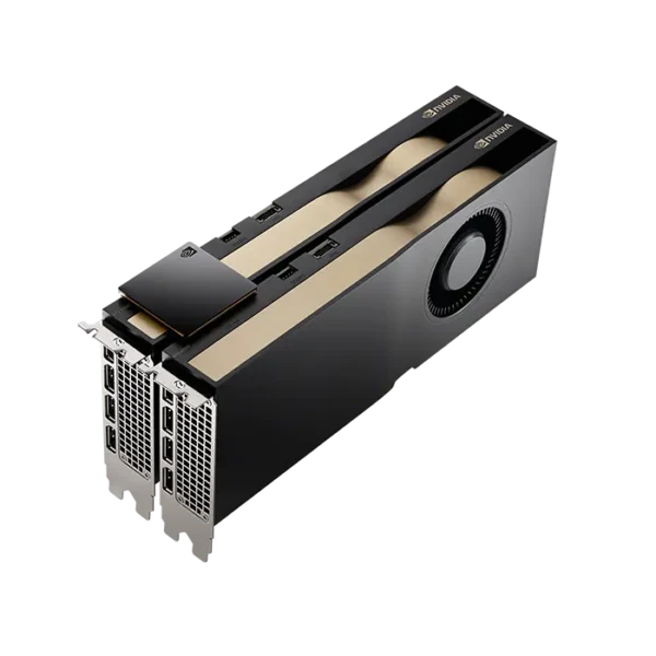
NVIDIA RTX A5500

- Type: Professional
- Process Node: 8 nm
- Memory Types: GDDR6
- Released Date: Mar 2022
The NVIDIA RTX A5500 was released in Mar 2022. This GPU was manufactured using 8nm process technology from Samsung, and it is based on Nvidia Ampere architecture. It maxed at a total power consumption of 230W. The RTX A5500 specs and all necessary information are in the table below.
Full Specifications And Prices
LAUNCH
| Announced | Mar 2022 |
| Available | Yes |
Board Design
| Type | Professional |
| Foundry | Samsung |
| TDP | 230W |
| Output Port | 4x DisplayPort 1.4a |
| Suggested PSU | 550W |
| Power Connectors | 1x 8-pin |
| Interface | PCIe 4.0 x16 |
| Generation | Quadro |
GPU Features
| CUDA | 8.6 |
| DirectX | 12 Ultimate (12_2) |
| OpenCL version | 3.0 |
| OpenGL | 4.6 |
| Shader Model | 6.6 |
| Vulkan version | 1.3 |
Graphics Processor
| Architecture | Ampere |
| Fabrication process | 8 nm |
| Die Size | 628mm² |
| GPU name | GA102 |
| Transistor count | 28,300 million |
Memory Specs
| Memory type | GDDR6 |
| Max size | 24GB |
| Max bandwidth | 768.0 GB/s |
| Memory Bus | 384bit |
| ECC Memory Support |
Clock Speeds
| Base Clock | 1695MHz |
| Boost Clock | 1695MHz |
| Memory Clock | 2000MHz |
Render Config
| L1 cache | 128 KB (per SM) |
| L2 cache | 6MB |
| Shading units | 10240 |
| TMUs | 320 |
| RT Cores | 80 |
| ROPs | 96 |
| GPU Major Cores | 80 |
| Tensor Cores | 320 |
Theoretical Performance
| FP16 (half) | 34.71 TFLOPS |
| FP32 (float) | 34.71 TFLOPS |
| FP64 (double) | 1085 GFLOPS |
| Texture Rate | 542.4 GTexel/s |
| Pixel Rate | 162.7 GPixel/s |
Reviews And Comments
Disclaimer Note
Disclaimer. We can not guarantee that the information on this page is 100% correct.


